Principal Investigator: Dr. Alan Mantooth
Advances in wide bandgap materials such as SiC and GaN have led to substantial advances in power semiconductor devices and are now positioned to dominate the next generation of power electronics replacing silicon devices. This research focuses on the creation and validation of analytical models for state-of-the-art GaN power devices.
The market share of GaN power devices is expected to reach a staggering $15.6 billion by 2022, mainly due to the growing demands in the power and energy sector, the communication infrastructure sector, and the power electronics market. GaN devices are expected to reduce overall energy conversion losses down to 1%, resulting in annual savings of nearly $40 billion in US revenues. A high-efficiency and green energy infrastructure is vital for reducing overall expenditures and reducing the carbon footprint of the electronics industry and the environment.The expected outcome from this fundamental research focuses on developing physics-based compact device models for circuit simulations that will help electronics engineers rapidly develop circuit designs and prototypes based on GaN devices. Impacts of this model will enable a side-by-side comparison of GaN and silicon devices at the design and analysis phase. This in turn will likely promote increased usage of GaN semiconductor technology. The models generated in this research will be open access and made publicly accessible on the NSF Industry/University Co-Operative Research Center website under the Grid-Connected Advanced Power Electronics Systems (GRAPES) center site.
Conventionally, the GaN device is a normally-on device. The device is shown in Fig.1 with its corresponding band diagram. GaN devices for power electronics applications are modified as shown in Fig. 2 with a p-type GaN gate and an AlGaN buffer layer. The discontinuity in polarization between the AlGaN barrier layer and p-GaN cap layer brings about the desired normally-off operation by lifting the conduction band above the Fermi-level.
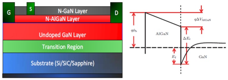
Figure 1: Classical GaN device operating as a normally-on transistor (i.e., a conducting path from source (S) to drain (D) exists with 0 V on the gate)
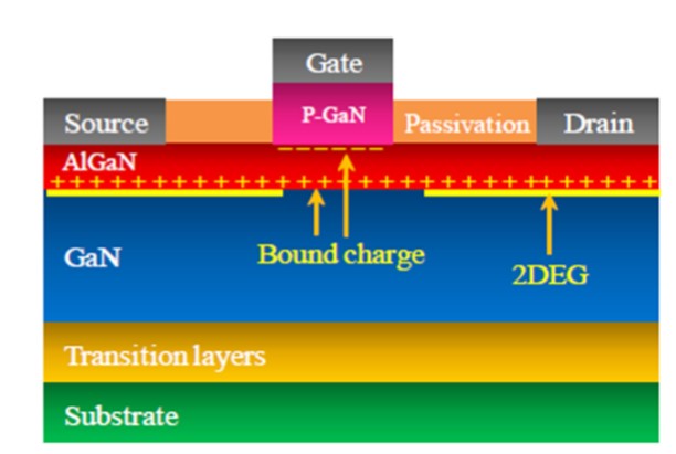
Figure 2: Cross-sectional structure of an AlGaN/GaN high electron mobility transistor (HEMT)modified for power applications with the p gate that shifts the band diagram such that the device is normally off
Recent Comments